🎸 游戏详情
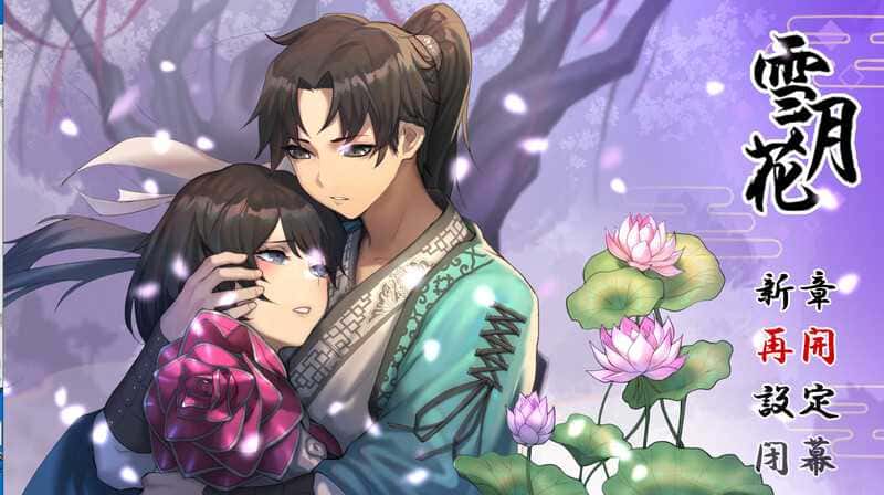
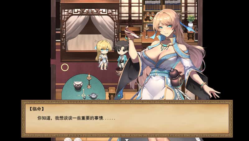
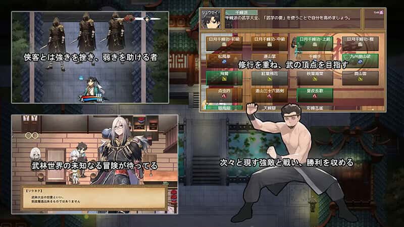
武侠是通过武术来实现正义的人。 这是一款武侠小说风格的RPG。 武侠世界叫做江湖,武侠地区叫做武林。 主角龙濑是一位冉冉升起的武侠人物,即使是他所属的森普派也非常重视他。 故事开始于龙井保护一个名为Hiiro的女孩,她从邪恶的教派逃脱。 他的师父凛美,他的妹妹徒弟濑树和喜朗。 在与这三位女英雄一起训练的日子里,龙濑参加了武术会议,以测试他的技能。
核心特色
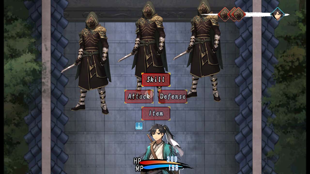
战斗系统
流畅的动作战斗
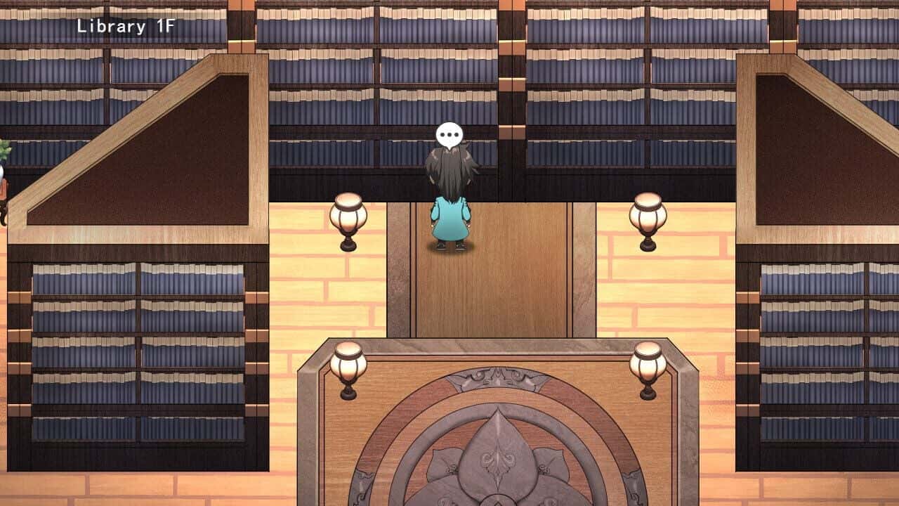
开放世界
自由探索冒险
多人合作
团队协作挑战
成就系统
丰富的奖励机制
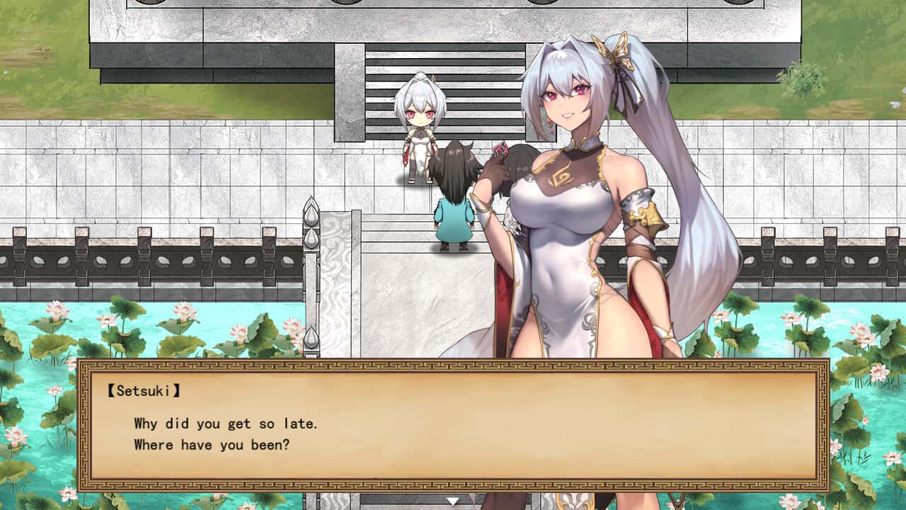
游戏截图
游戏数据
9.4
平均评分
2.3M
总下载量
900K
活跃玩家
系统要求
操作系统
Windows 10+
内存
8GB RAM
显卡
GTX 1060
存储空间
50GB